About Me
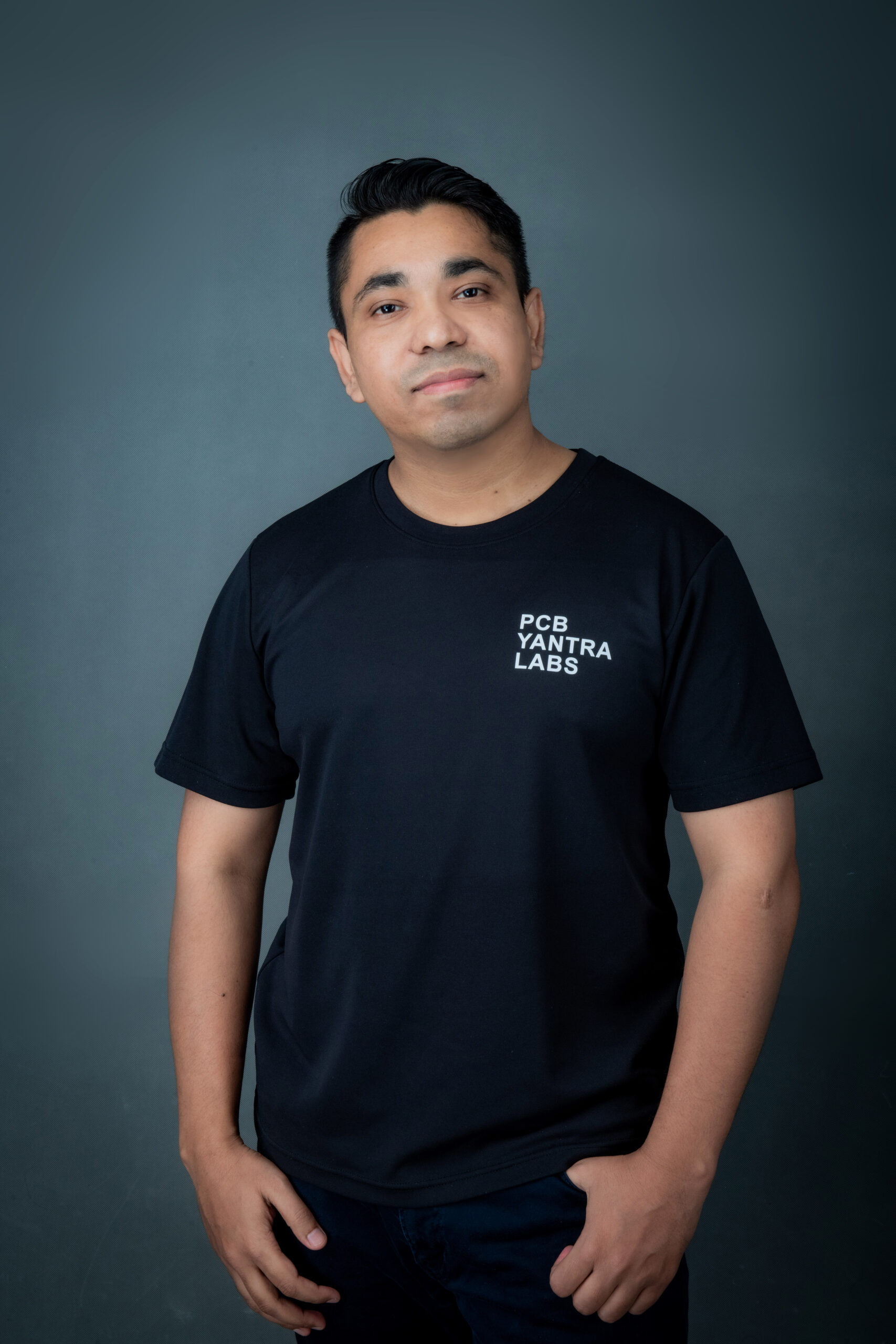
SOMNATH SINGH
Founder of
''PCB Yantra Labs"
( SI/PI Engineer )
YouTuber
Hardware Design Educator
Architecting High-Performance Electronics Systems
My journey began with Project STUDSAT-2, designing aerospace-grade power systems. This foundation in reliability now drives my work in Hsinchu, Taiwan, where I architect complex, multi-layer high-speed systems
After refining my expertise through a Master’s at National Tsing Hua University, I have spent the last several years embedded in the heart of Taiwan’s semiconductor ecosystem. I specialize in translating complex, theoretical system requirements into manufacturable, high-reliability hardware. My work focuses on the intersection of Signal Integrity (SI) and Power Integrity (PI), ensuring that even the most dense designs operate with surgical precision
Bridging the Gap Between Research and Physical Reality
Through PCByantra Labs, I focus on the ‘physics-first’ approach to hardware—ensuring that every trace and component is optimized for signal integrity and long-term system stability
Hardware is where physics meets the real world. I believe in a simulation-driven design process—tackling EMI/EMC challenges and thermal constraints before the first board is ever fabricated. My goal with every project is to reduce costly re-spin cycles and deliver ‘first-pass’ success. Through PCByantra Labs, I provide the high-level architectural oversight needed to turn ambitious research into stable, physical platforms.
Core Technical Domains
Specializing in the full-cycle implementation of high-density electronic systems, from initial schematic and 3D modeling to physical fabrication and bench-level validation.
Work Experience
Focus: Leading the architecture of high-speed digital systems and complex hardware designs.
- Specialization: Implementing 8+ layer PCB layouts with a physics-first approach to ensure Signal and Power Integrity (SI/PI) for high-bandwidth interfaces like LPDDR4 SDRAM and PCIe.
Focus: Managed full-lifecycle development of professional electronic boards, from layout planning to physical hardware implementation.
Specialization: Expert operation of EDA tool chains for PCB Layout, circuit board schematic design, and advanced routing in a high-demand R&D environment.
Focus: Architected Electronic Power Systems (EPS) for small satellite missions, including generation and storage unit boards.
Impact: Coordinated hardware prototypes with leading aerospace scientists and provided technical mentorship to over 150 students in systems engineering.
Focus: Bridged the gap between theoretical NanoEngineering research and physical hardware during my Master’s at National Tsing Hua University.
Specialization: Developed high-performance interface circuits and focused on translating complex academic concepts into robust, manufacturable systems.
Focus: Established PCByantra Labs to document a decade of hardware evolution and share high-level engineering insights with the global community.
Impact: Bridging the gap between theory and practice through content creation and technical guidance for the next generation of hardware designers.
Join the PCB Yantra Network
Subscribe to receive technical deep-dives on high-speed PCB design, signal integrity analysis, and professional hardware engineering insights.