
About Me
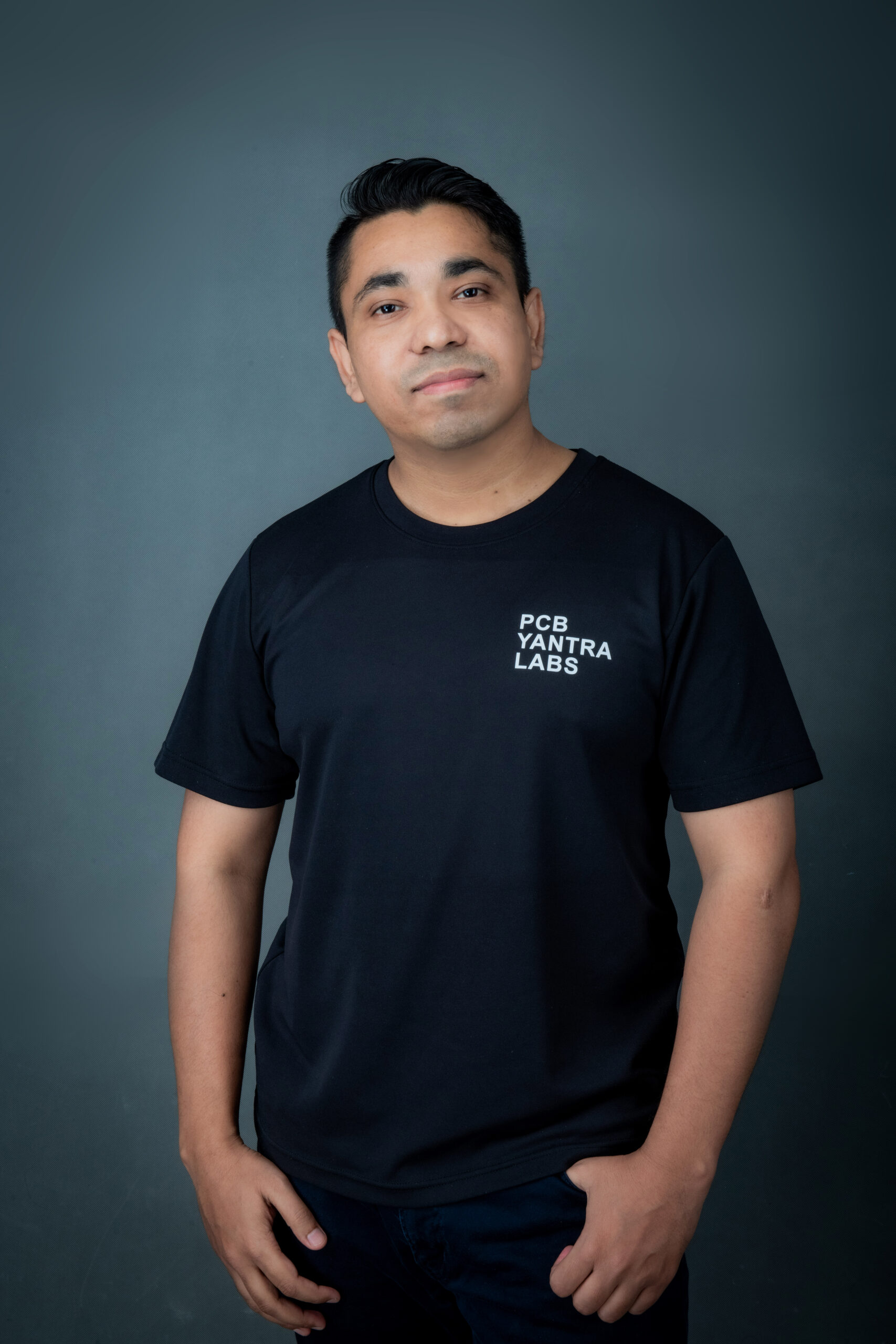
Hardware Design Engineer
& YouTube Educator
It started with a small satellite’s power board. At STUDSAT-2, India’s twin nano-satellite mission, I helped lead the Electrical Power Subsystem and designed my first PCB from scratch, entirely self-taught. That same drive carried me through a Master’s at National Tsing Hua University and into Taiwan’s hardware industry. Since then I’ve been turning raw ideas into working hardware, including a Lidar Motherboard I helped carry through bring-up, testing, and several rework cycles.
That bring-up-and-rework grind taught me how much of a board’s behavior lives in physics the schematic never shows. So now that same drive is aimed at mastering Signal and Power Integrity — the discipline that decides whether a high-speed board actually works, or just looks like it should.
Every board eventually answers to physics. I believe each design decision — stackup, trace geometry, decoupling — should trace back to that physics, not guesswork. That’s the principle behind PCB Yantra Labs, where I teach what I find: real boards, real debugging, real physics.
My goal on every project is to catch problems on the bench and in simulation before they ever reach fabrication, cutting the costly re-spin cycles that come from missing them. I’ve lived through exactly that cost myself, so I know why the standard matters — and I’m building toward it deliberately, through hands-on board work, structured self-study, and sharing every lesson I learn.
Core Technical Domains
Work Experience
Research Assistant
- Architecture: Designing piezoelectric (AlN) MEMS accelerometers and their mixed-signal PCB interface circuitry.
- Impact: Engineering novel proof-mass geometries to optimize eigenfrequency, extending my Master’s thesis work toward a forthcoming publication.
+ Read Context
Returned to the RF MicroSystems Lab in 2026 to deepen this MEMS structural research, building on an earlier 2023 stint designing the interface circuit for a MEMS gyroscope and remote collaboration with the same lab through 2025.
Hardware R&D Design Engineer
- Architecture: Second design engineer on a Lidar motherboard’s core carrier board, built around a Xilinx daughterboard.
- Impact: Owned the Ethernet interface routing — a skill built on the job — and helped carry the board through bring-up and rework to reliable operation.
+ Read Context
Working under a lead engineer, with two junior engineers on the wider team, I handled roughly 60% of the PCB layout myself — including Ethernet routing I’d never done before this project — while the lead engineer took on the more complex remaining portion. Multiple rework and debugging cycles followed before the board reached stable operation.
Core Leader / Systems Engineer
- Architecture: Led the Electrical Power Subsystem (EPS) for STUDSAT-2, India’s twin nano-satellite mission, designing its power generation and storage boards from scratch, self-taught.
- Impact: Mentored 50+ undergraduate engineers across a seven-college consortium as core leader, coordinating final-year projects with ISRO scientists’ technical guidance.
+ Read Context
This is where I first taught myself PCB design, driven by the exacting physics of orbital hardware — the same board is now featured on the Capabilities page.